Differences
This shows you the differences between two versions of the page.
| Both sides previous revision Previous revision Next revision | Previous revision | ||
|
boards:wio-e5 [2022/12/29 02:53] darron |
boards:wio-e5 [2022/12/31 19:18] (current) darron [STM32WLE5JC] |
||
|---|---|---|---|
| Line 9: | Line 9: | ||
| </ | </ | ||
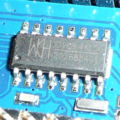
| - | STM32WLE5JC | + | This board has a package containing a STM32WLE5JC |
| + | |||
| + | The MCU does not contain a FPU, only the mandatory DSP for m4 | ||
| + | cores, but it does have an embedded radio, it appears to be an SX1262. | ||
| + | |||
| + | |||
| + | ===STM32WLE5JC=== | ||
| + | |||
| + | RAM is in two 32K banks, which may be addressed separately or contiguously. The | ||
| + | second bank has extended features when used separately. | ||
| < | < | ||
| 256K FLASH | 256K FLASH | ||
| - | 64K RAM (2 banks of 32K) | + | 64K RAM |
| AES 256 | AES 256 | ||
| LoRa | LoRa | ||
| - | FPU not present | ||
| </ | </ | ||
| + | |||
| + | There is a warning in the reference manual on page 185 of RM0461 Rev 5: | ||
| + | |||
| + | "The SMPS needs a clock to be functional. If for any reason this clock stops, | ||
| + | the device may be destroyed." | ||
| + | |||
| + | I probably would not have bothered with this board had I read the above warning beforehand. | ||
| + | Who designs a MCU that can self destruct if a bit doesn' | ||
| + | |||
| ===Test=== | ===Test=== | ||
| Line 66: | Line 83: | ||
| Warning: This process will erase the write protected firmware and this | Warning: This process will erase the write protected firmware and this | ||
| is non-recoverable. | is non-recoverable. | ||
| + | |||
| + | NB when removing protection, the device will need to be power cycled afterwards. | ||
| < | < | ||
| Line 142: | Line 161: | ||
| Connecting to the board using JLinkExe will remove protection and erase | Connecting to the board using JLinkExe will remove protection and erase | ||
| the firmware but this can also be done using a standalone tool. | the firmware but this can also be done using a standalone tool. | ||
| + | |||
| + | NB when removing protection, the device will need to be power cycled afterwards. | ||
| < | < | ||
| Line 179: | Line 200: | ||
| ===Clock=== | ===Clock=== | ||
| - | HSE 32MHz TCXO | + | On reset the MCU uses the MSI clock at 4 MHz. |
| + | |||
| + | ==HSE== | ||
| + | |||
| + | 32MHz TCXO | ||
| < | < | ||
| Line 185: | Line 210: | ||
| </ | </ | ||
| - | LSE 32.768KHz | + | ==LSE== |
| + | 32.768KHz | ||
| ===Antenna=== | ===Antenna=== | ||
| Line 232: | Line 258: | ||
| [[https:// | [[https:// | ||
| + | [[https:// | ||