Differences
This shows you the differences between two versions of the page.
| Both sides previous revision Previous revision Next revision | Previous revision | ||
|
boards:rkp28sb [2014/12/16 09:07] darron |
boards:rkp28sb [2020/12/28 12:36] (current) |
||
|---|---|---|---|
| Line 1: | Line 1: | ||
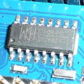
| - | ==== RK Education | + | ==== RKP28sb ==== |
| - | {{ :wiki:k8048: | + | <wrap right> |
| + | {{:boards: | ||
| + | </ | ||
| The RKP28sb is a USB development board for the PIC18F2550 or equivalent. | The RKP28sb is a USB development board for the PIC18F2550 or equivalent. | ||
| - | == Documentation at RK Education == | + | === PIC18F2550 pinout |
| - | [[http:// | + | |
| - | [[http:// | + | |
| - | [[http:// | + | |
| - | + | ||
| - | == PIC18F2550 pinout == | + | |
| < | < | ||
| !MCLR VPP RE3 1-----28 RB7 KBI3 PGD | !MCLR VPP RE3 1-----28 RB7 KBI3 PGD | ||
| Line 26: | Line 23: | ||
| VUSB | VUSB | ||
| </ | </ | ||
| - | == I/O == | + | === I/O === |
| < | < | ||
| J9 ICSP | J9 ICSP | ||
| - | ------- | + | ------- |
| 1:VPP !MCLR VPP RE3 | 1:VPP !MCLR VPP RE3 | ||
| 2: | 2: | ||
| Line 41: | Line 38: | ||
| 1:RST !MCLR VPP RE3 1:RC0 RC0 T1OSO T13CKI | 1:RST !MCLR VPP RE3 1:RC0 RC0 T1OSO T13CKI | ||
| 2:3V3 +3V3 | 2:3V3 +3V3 | ||
| - | 3:5V +5V | + | 3:5V +5V J8 J4 |
| - | 4:GND | + | 4:GND |
| - | 5:GND | + | 5:GND |
| - | 6:VIN | + | 6:VIN |
| - | | + | |
| J3 ANALOGUE | J3 ANALOGUE | ||
| ----------- | ----------- | ||
| Line 54: | Line 51: | ||
| 5: | 5: | ||
| 6: | 6: | ||
| + | |||
| + | SCK on J8 connects to LED D3 | ||
| </ | </ | ||
| + | === Power === | ||
| + | |||
| + | Power may be applied through the power jack or the power header. There are two LDOs and a jumper is used to select the MCU voltage between 3V3 or 5V. When applying 5V on the power header, the 3V3 LDO is still utilised so it may be selected. | ||
| + | |||
| + | When using the power jack socket, the switch will turn the board on and off, as it | ||
| + | feeds the 5V LDO. | ||
| + | |||
| + | There is a VUSB selection jumper which may power this pin if the PIC internal regulator is disabled. For PICs that are not USB, remove the jumper and use this a method of accessing pin 14. | ||
| + | |||
| + | === Resources === | ||
| + | [[https:// | ||
| + | [[https:// | ||