Differences
This shows you the differences between two versions of the page.
| Both sides previous revision Previous revision Next revision | Previous revision | ||
|
boards:opi0 [2017/01/11 04:18] darron [GPIO] |
boards:opi0 [2020/08/05 04:53] (current) darron [Pickle Microchip PIC ICSP] |
||
|---|---|---|---|
| Line 2: | Line 2: | ||
| <wrap right> | <wrap right> | ||
| {{: | {{: | ||
| - | \\ \\ | ||
| - | {{: | ||
| </ | </ | ||
| The Orange Pi Zero is a Linux compatible computer with high speed GPIO. | The Orange Pi Zero is a Linux compatible computer with high speed GPIO. | ||
| + | It contains four ARMv7 CPU cores present in the AllWinner H2+ (cost reduced H3) system on a chip. | ||
| + | |||
| + | A debian derived distribution of Linux called Armbian works on this device. It's important | ||
| + | to install this on a class 10 microsd card and not a class 4 which has incredibly poor | ||
| + | write performance. A sandisk ultra micro SDHC 10x works well. | ||
| === GPIO === | === GPIO === | ||
| - | The board has a [[boards: | + | The board has a [[boards: |
| - | Whilst the GPIO is compatible with the RPi note the orientation. | + | Whilst the GPIO header |
| < | < | ||
| Line 29: | Line 32: | ||
| </ | </ | ||
| - | This is the relationship between the OPi0 IO, H2+/H3 I/O, the Linux sysfs interface and alternate pin function. | + | This is the relationship between the Orange Pi Zero GPIO pins, H2+/H3 I/O, Linux sysfs interface and the H2+/ |
| - | ^Pin ^H2+/H3 I/O ^sysfs ^Alt | | + | ^Pin ^H2+/H3 I/O ^sysfs ^ALT |
| | 3 | PA12 | 12 | SDA | | | 3 | PA12 | 12 | SDA | | ||
| | 5 | PA11 | 11 | SCK | | | 5 | PA11 | 11 | SCK | | ||
| Line 38: | Line 41: | ||
| | 10 | PG7 | 199 | RxD | | | 10 | PG7 | 199 | RxD | | ||
| | 11 | PA1 | 1 | RxD | | | 11 | PA1 | 1 | RxD | | ||
| - | | 12 | PA7 | 7 | + | | 12 | PA7 | 7 | |
| | 13 | PA0 | 0 | TxD | | | 13 | PA0 | 0 | TxD | | ||
| | 15 | PA3 | 3 | CTS | | | 15 | PA3 | 3 | CTS | | ||
| Line 52: | Line 55: | ||
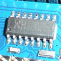
| === Pickle Microchip PIC ICSP === | === Pickle Microchip PIC ICSP === | ||
| + | <wrap right> | ||
| + | {{: | ||
| + | </ | ||
| - | Along with USB serial we can use the OPi0 GPIOs to program PICMicros using [[projects: | + | We can use the Orange Pi Zero GPIOs to program PICMicros using [[projects: |
| - | Memory mapped I/O can be used to drive the GPIOs, however, the [[projects: | + | The [[projects: |
| + | and uses the same numbering. | ||
| == Low Voltage Programming with VPP at 3V3 == | == Low Voltage Programming with VPP at 3V3 == | ||
| - | Low voltage ICSP at 3V3 can be performed directly from the OPi0 GPIOs. | + | Low voltage ICSP at 3V3 can be performed directly from the GPIOs. |
| - | The following connections refer to the OPi0 GPIO header. Ensure that power is only ever applied from GPIO 3V3 on PIN 1 and never 5V. | + | The following connections refer to the GPIO header. Ensure that power is only ever applied from GPIO 3V3 on PIN 1 and never 5V. |
| - | Single common data I/O connection (OPi0 or GPIO bit-bang driver) | + | Single common data I/O connection (OPI0 or GPIO bit-bang driver) |
| < | < | ||
| OPi0 H2+/ | OPi0 H2+/ | ||
| Line 72: | Line 79: | ||
| | | ||
| | | | | ||
| - | | + | |
| - | | + | |
| - | | + | |
| - | | + | |
| - | | | + | |
| - | /// | + | |
| (R1) 10K !MCLR pull-up | (R1) 10K !MCLR pull-up | ||
| - | (R2) 10K where appropriate (PGM is not present on all devices). | + | (R2..R4) 390R. |
| - | (R3..R6) 470R. | + | |
| + | DEVICE=OPI0 | ||
| + | or | ||
| + | DEVICE=GPIO-BB | ||
| + | IFACE=/ | ||
| </ | </ | ||