Differences
This shows you the differences between two versions of the page.
|
boards:k8048 [2014/12/17 14:17] darron |
boards:k8048 [2015/03/22 21:55] |
||
|---|---|---|---|
| Line 1: | Line 1: | ||
| - | ==== Velleman K8048 ==== | ||
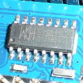
| - | {{ : | ||
| - | == Serial Interface == | ||
| - | The Velleman programmer board has the following serial interface | ||
| - | characteristics (D-SUB-9): | ||
| - | |||
| - | < | ||
| - | | ||
| - | | ||
| - | 1 2 3 4 5 | ||
| - | 6 7 8 9 | ||
| - | |||
| - | | ||
| - | | ||
| - | | ||
| - | | ||
| - | | ||
| - | 6:DSR | ||
| - | | ||
| - | | ||
| - | 9:RI | ||
| - | </ | ||
| - | |||
| - | Although the interface connects to the serial port, it doesn' | ||
| - | the RS-232 serial protocol and instead I/O is performed with bit banging. | ||
| - | |||
| - | Data output bits are sent through the DTR line and clocked on the falling | ||
| - | edge of RTS. | ||
| - | |||
| - | The Tx line is utilised to enable the application of the high programming | ||
| - | voltage on !MCLR/VPP and not for sending data bits. | ||
| - | |||
| - | Data input bits are read from the CTS line using the same clock as for | ||
| - | output with the data output line taken high for correct circuit operation. | ||
| - | |||
| - | |||
| - | == Socket Cross Reference == | ||
| - | |||
| - | < | ||
| - | | ||
| - | | ||
| - | | ||
| - | | ||
| - | | ||
| - | | ||
| - | | ||
| - | | ||
| - | | ||
| - | | ||
| - | |||
| - | | ||
| - | | ||
| - | | ||
| - | | ||
| - | |||
| - | | ||
| - | | ||
| - | | ||
| - | | ||
| - | | ||
| - | |||
| - | | ||
| - | | ||
| - | |||
| - | | ||
| - | | ||
| - | |||
| - | | ||
| - | | ||
| - | | ||
| - | | ||
| - | | ||
| - | | ||
| - | | ||
| - | | ||
| - | | ||
| - | </ | ||
| - | |||
| - | == ICSP == | ||
| - | |||
| - | < | ||
| - | SK3 is an ICSP port, the pins are arranged as follows: | ||
| - | |||
| - | ICSP | ||
| - | | ||
| - | 5 4 3 2 1 | ||
| - | |||
| - | 1:VPP 12V | ||
| - | 2:VDD 5V | ||
| - | | ||
| - | 4:PGD | ||
| - | 5:PGC | ||
| - | </ | ||
| - | |||
| - | < | ||
| - | ICSP voltage levels (No chip installed, no D-SUB-9 connection) | ||
| - | | ||
| - | |||
| - | | ||
| - | |||
| - | | ||
| - | | ||
| - | | ||
| - | | ||
| - | | ||
| - | |||
| - | | ||
| - | |||
| - | | ||
| - | | ||
| - | | ||
| - | | ||
| - | | ||
| - | |||
| - | | ||
| - | |||
| - | | ||
| - | | ||
| - | | ||
| - | | ||
| - | | ||
| - | </ | ||