Differences
This shows you the differences between two versions of the page.
| Both sides previous revision Previous revision Next revision | Previous revision | ||
|
projects:esp [2015/02/04 12:32] darron [PCF8591] |
projects:esp [2017/01/12 22:44] (current) |
||
|---|---|---|---|
| Line 5: | Line 5: | ||
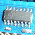
| {{: | {{: | ||
| </ | </ | ||
| - | |||
| - | __This project page is under construction__ | ||
| This project adds three I2C devices to an [[: | This project adds three I2C devices to an [[: | ||
| Line 12: | Line 10: | ||
| The three devices are a Microchip MCP23016 digital I/O expander, NXP PCF8591 ADC/DAC and Microchip 24LC512 EEPROM. | The three devices are a Microchip MCP23016 digital I/O expander, NXP PCF8591 ADC/DAC and Microchip 24LC512 EEPROM. | ||
| - | These were chosen because they add useful capabilities to the ESP-01 or RPi and all three are available in DIP format from CPC in the United Kingdom. | + | These were chosen because they add useful |
| + | You may also consider adding an I2C RTC to this project and perhaps it shall be updated to include one at a later time. | ||
| === Schematic === | === Schematic === | ||
| + | |||
| + | The circuit is expected to be used with either an ESP-01 attached and with its UART connected to a computer to load in scripts, else without an ESP-01 and with the I2C lines connected to a Raspberry Pi. | ||
| {{: | {{: | ||
| + | It should be reasonably simple to construct on stripboard. Tripad board will be used to demonstrate this at a later time. | ||
| === I2C bus === | === I2C bus === | ||
| + | |||
| + | The I2C bus is simple affair with only two lines required for its operation. This is perfect for the ESP-01 module which only has two GPIOs exposed on its header pins. For the Raspberry Pi, there are two I2C buses, but only one is normally available. | ||
| ^Address ^Device | | ^Address ^Device | | ||
| Line 24: | Line 28: | ||
| |0x48 |PCF8591| | |0x48 |PCF8591| | ||
| |0x50 |24LC512| | |0x50 |24LC512| | ||
| + | |||
| + | These addresses are the defaults for all three devices with the address pins tied low. Multiple devices of the same type are easily accommodated on the I2C bus but this is not demonstrated here. | ||
| Probing the bus on the RPi with [[: | Probing the bus on the RPi with [[: | ||
| Line 39: | Line 45: | ||
| </ | </ | ||
| === MCP23016 === | === MCP23016 === | ||
| + | |||
| + | The MCP23016 is general purpose digital I/O expander. There are more modern and faster varieties of this device but as yet they are not available at CPC. | ||
| ^Control ^Register ^Function | | ^Control ^Register ^Function | | ||
| Line 50: | Line 58: | ||
| To use the MCP23016 first set the GPIO direction register. Microchip use 1 for input and 0 for output. After that you can either read the input register or write to the output register. | To use the MCP23016 first set the GPIO direction register. Microchip use 1 for input and 0 for output. After that you can either read the input register or write to the output register. | ||
| - | [[: | + | == ESP-01 NodeMcu == |
| - | Here we clear the output latch, set GP0.0 to an output, then set the pin high on the RPi. | + | The NodeMcu firmware can be controlled via a serial console. This can be a manual operation else with a specially written tool for the job: eSPY. |
| + | |||
| + | First we need to fetch eSPY, and then build it. The examples for eSPY on this page come with the eSPY source. | ||
| < | < | ||
| - | i2cset -y 1 0x20 2 0 | + | hg clone http:// |
| - | i2cset -y 1 0x20 6 0xFE | + | cd epsy |
| - | i2cset -y 1 0x20 2 1 | + | make |
| </ | </ | ||
| - | The equivalent code for NodeMcu LUA on the ESP-01 is. | + | This example script blinks an LED attached to the MCP23016 GP0.0 pin. |
| < | < | ||
| #!espy / | #!espy / | ||
| Line 96: | Line 106: | ||
| </ | </ | ||
| - | It is run via eSpy (to be documented). | + | The script comes with the eSPY application and can be demomstrated like this. |
| < | < | ||
| ./mcp.esp | ./mcp.esp | ||
| - | > > > > > > > >> >> >> >> >> >> > > > > > >> >> >> >> >> >> >> on | ||
| off | off | ||
| on | on | ||
| Line 107: | Line 116: | ||
| </ | </ | ||
| - | Here on the RPi we set GP1.0 as an input then read it twice. The first read is with GP1.0 taken | + | == RPi == |
| + | |||
| + | [[: | ||
| + | |||
| + | Here we clear the output latch, set GP0.0 to an output, then set the pin high on the RPi. | ||
| + | < | ||
| + | i2cset -y 1 0x20 2 0 | ||
| + | i2cset -y 1 0x20 6 0xFE | ||
| + | i2cset -y 1 0x20 2 1 | ||
| + | </ | ||
| + | |||
| + | Now on the RPi we set GP1.0 as an input then read it twice. The first read is with GP1.0 taken | ||
| low and the second read with GP1.0 taken high. | low and the second read with GP1.0 taken high. | ||
| < | < | ||
| Line 120: | Line 140: | ||
| === PCF8591 === | === PCF8591 === | ||
| + | |||
| + | The PCF8591 combines 4 analogue inputs and a single analogue output. The inputs can be more than simple input channels but this isn't looked at here. | ||
| + | |||
| ^Control ^Register | ^Control ^Register | ||
| |0 | channel 0 |Read ADC 0| | |0 | channel 0 |Read ADC 0| | ||
| Line 129: | Line 152: | ||
| To write to the DAC, we set the control to 64 and write a value between 0 and 255 which represents 0 to VREF volts on the output pin. | To write to the DAC, we set the control to 64 and write a value between 0 and 255 which represents 0 to VREF volts on the output pin. | ||
| - | Using [[: | + | To read from an ADC, we first send a control representing |
| - | < | + | |
| - | i2cset -y 1 0x48 64 0 | + | If we are using the DAC, then we must also set the analog OE bit else the DAC will be disabled. |
| - | i2cset -y 1 0x48 64 128 | + | |
| - | i2cset | + | == ESP-01 NodeMcu == |
| - | </ | + | |
| - | With NodeMcu LUA script, a simple ramp demo can be achieved like this. | + | A simple ramp demo can be achieved like this with NodeMcu on the ESP-01. |
| < | < | ||
| #!espy / | #!espy / | ||
| Line 166: | Line 188: | ||
| </ | </ | ||
| - | When the script is run with eSPY we can see the DAC output ramp up and a running | + | When the script is run with eSPY we can see the DAC output ramp up with a running |
| < | < | ||
| - | > > > > > > > >> >> >> >> >> >> > > >> | + | 0 |
| - | >> >> >> >> | + | |
| 10 | 10 | ||
| 20 | 20 | ||
| Line 179: | Line 200: | ||
| </ | </ | ||
| - | To read from an ADC, we first send a control representing the channel, then we perform two reads. The first read starts the conversion process and the second read fetches the result (this also starts another conversion). | + | == RPi == |
| - | If we are using the DAC, then we must also set the analog OE bit else the DAC will be disabled. | + | Using [[: |
| + | < | ||
| + | i2cset -y 1 0x48 64 0 | ||
| + | i2cset -y 1 0x48 64 128 | ||
| + | i2cset -y 1 0x48 64 255 | ||
| + | </ | ||
| With a potentiometer connected to AIN0 a reading was made on the RPi. | With a potentiometer connected to AIN0 a reading was made on the RPi. | ||
| Line 197: | Line 223: | ||
| I2C EEPROMs have varied addressing schemes. The simplest is a 8-bit address offset, another one where a block selection is made with an I2C address and a byte selection is made with an 8-bit address offset. Yet another, where the I2C address is fixed but it now has a 16-bit address offset and lastly one with both of the last methods combined. | I2C EEPROMs have varied addressing schemes. The simplest is a 8-bit address offset, another one where a block selection is made with an I2C address and a byte selection is made with an 8-bit address offset. Yet another, where the I2C address is fixed but it now has a 16-bit address offset and lastly one with both of the last methods combined. | ||
| - | Here we will demonstrate the 24LC512 | + | The 24LC512 |
| - | On the RPi we can reset the internal address pointer of the chip to 0 like this. | + | == ESP-01 NodeMcu == |
| - | < | + | |
| - | i2cset | + | |
| - | </ | + | |
| - | + | ||
| - | To read, we first write an address to start at then begin reading, if we keep reading the address is auto-incremented. | + | |
| - | < | + | |
| - | i2cset -y 1 0x50 0 0 | + | |
| - | i2cget -y 1 0x50 | + | |
| - | 0x55 | + | |
| - | i2cget -y 1 0x50 | + | |
| - | 0xaa | + | |
| - | </ | + | |
| - | + | ||
| - | If we want to write to a location we send the address followed by the byte of data. | + | |
| - | < | + | |
| - | i2cset -y 1 0x50 0 0 0xEE i | + | |
| - | i2cset -y 1 0x50 0 0 | + | |
| - | i2cget -y 1 0x50 | + | |
| - | 0xee | + | |
| - | </ | + | |
| On the ESP-01 we can use this NodeMcu LUA script to read the EEPROM. | On the ESP-01 we can use this NodeMcu LUA script to read the EEPROM. | ||
| Line 256: | Line 262: | ||
| </ | </ | ||
| - | Here the script is executed using eSPY (to be documented). | + | Here the script is executed using eSPY. |
| < | < | ||
| ./ | ./ | ||
| - | > > > > > > > >> >> >> >> >> >> >> >> >> >> >> > > > > 238 | + | 238 |
| </ | </ | ||
| - | eSPY is still being developed and as yet doesn' | + | == RPi == |
| + | |||
| + | On the RPi we can reset the internal address pointer of the chip to 0 like this. | ||
| + | < | ||
| + | i2cset -y 1 0x50 0 0 | ||
| + | </ | ||
| + | |||
| + | To read, we first write an address to start at then begin reading, if we keep reading the address | ||
| + | < | ||
| + | i2cset -y 1 0x50 0 0 | ||
| + | i2cget -y 1 0x50 | ||
| + | 0x55 | ||
| + | i2cget -y 1 0x50 | ||
| + | 0xaa | ||
| + | </ | ||
| + | |||
| + | If we want to write to a location we send the address followed by the byte of data. | ||
| + | < | ||
| + | i2cset -y 1 0x50 0 0 0xEE i | ||
| + | i2cset -y 1 0x50 0 0 | ||
| + | i2cget -y 1 0x50 | ||
| + | 0xee | ||
| + | </ | ||
| This overview gives enough information to use the device at a byte level, read the [[# | This overview gives enough information to use the device at a byte level, read the [[# | ||
| Line 270: | Line 298: | ||
| [[http:// | [[http:// | ||
| [[http:// | [[http:// | ||
| + | |||